2015年9月8日星期二

Semi-flexible PCB technology


With simple depth-milling a standard printed circuit board can be prepared for flexible installations. So called "semi-flexible" printed circuits are offering a cost-efficient solution. They save connectors and increase reliability while decreasing size of the application and time needed for assembly. Semi-flexible PCBs are the perfect solution if you have flex-to-install requirements only and there is no dynamic bending during operation.


Often layout designers are reluctant to upgrade from a standard PCB with connectors to a notoriously expensive rigid-flexible printed circuit. The advantages are immense, but so are the costs and the layout requirements compared to standard PCBs. Many times this "jump" from standard technology to a high-tech segment is not necessary. Many printed circuits do not require dynamic bending capabilities in operation but only need to be fit into the housing neatly. This is called a "flex-to-install" requirement and here semi-flex offers a really cost-saving alternative technology.


Production of a semi-flexible PCB is identical with the manufacturing process of standard printed circuits. Semi-flexilbe boards can be produced as single-layer, double-layer or multilayer PCBs. With the exemption of a special solder mask that sustains bending, the materials are also identical to standard printed circuits. The only difference happens at the end of the production process when dedicated bending areas are milled down by z-axis routing. The remaining material can be bend and is thin enough to only carry the copper traces and little base material.


Design and installation of semi-flexible PCBs require some attention and modifications:

1.      The PCB should only be bend with copper on the outside of the bending area.

2.      Open copper structures, pads, annular rings or vias in the rigid part of the PCB should have a distance of at least 1mm from the bending area. In special cases 0,8mm are okay, too. The semi-flexible are cannot contain any vias, drills or open copper structures. The transition area from flexible to rigid should have a radius of 5mm or an obstuse angle. Trace-to-outline distance in the semi-flexible area should be minimum 0,30mm.


3.      The maximum bending radius depends on the lenght of the semi-flexible area:


4.      Currently, semi-flexible PCBs are possible up to 8 layers, while only one outer layer can be "semi-flexible" per bending area.


Baggio WANG FAN
-----------------------------------------------------------
SHENZHEN JAAPSON TECHNOLOGY CO LTD
Building 2, Tongfuyu Industrial Park,Shenzhen, China, 518104
Tel: 86-755-82596922
Fax:86-755-82596922/82596923
skype: baggiowang0214
baggio.wang@funsunpcb.com
baggio@jaapson-pcb.com
www.jaapsonpcb.com
 
JAAPSON, The Expert in HDI Multi-layer PCBs

2015年9月7日星期一

The Advantages of COB technology in LED


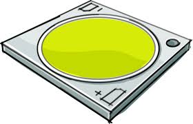
COB (known as Chip-on-Board) is semi-conductor assembly technology where micro-chip also known as die is electrically interconnected instead of using traditional assembly process or individual IC packaging on the final product board. The general term meaning of this technology is direct chip attachment also refereeing to DCA. In DCA many kinds are available as substrate in form of ceramic glass or ceramic substrate which has substances of excellent dielectric and thermal property. It is also available in form of flex substrate, which exhibits bendable ability. Other names are known as COG (chip-on-glass) or COF (chip-on-flex).


COB process consists of three main categories to perform when manufacturing the Chip-on-Board. The first process is 'die mount or die attach', the second is 'wire bonding' and lastly 'the encapsulation of die wires'. 


In many COB assembly technology, FCOB(flip-chip-on-board) have chips facing downward on the board and does not require wire bonding which employs chip which the bond pads are pop up and it connects directly to pads on the board. It is necessary to underfill flip-chip on active surface to protect bumps from chemical and thermo-mechanical damage.


 In context of COB manufacturing process, 1) 'die attach' consists of applying die attach holding to board or substrate mounting chip or die over die attach materials. 2) For wire bonding, thermosonic (Au or Cu) ball bending and ultrasonic (Al) wedge bending are used to connect wires between die and substrate. Last part the encapsulation is done dispensing chemical liquid (usually epoxy) over die and wires. Die and bond wires are encapsulated to protect chemical and mechanical damage.


The advantages of COB include:
Better performance due to deceased interconnection between length and resistance.
And better protection against reverse engineering;
Reduced space and cost;
Shorter time to the market.
Higher reliability with better heat dispatch and small number of solder joint.


Applications
LED Backlight for LCD TV
LED Front light for E-Book
Agriculture & Horticulture Lighting
Street & Parking Lot Lighting

Invention
Reflective Pocket in PCB for LED Die Attachment (COB)
Patent pending

Advantages
Improved output efficiency of LED lighting
Avoid photonic absorption and scattering over the pocket wall


Baggio WANG FAN
-----------------------------------------------------------
SHENZHEN JAAPSON TECHNOLOGY CO LTD
Building 2, Tongfuyu Industrial Park,Shenzhen, China, 518104
Tel: 86-755-82596922
Fax:86-755-82596922/82596923
skype: baggiowang0214
baggio.wang@funsunpcb.com
baggio@jaapson-pcb.com
www.jaapsonpcb.com
JAAPSON, The Expert in HDI Multi-layer PCBs

2015年9月1日星期二

Best of Free PCB Design Software


Do you need a free PCB design software or tool to put in practice the new electronic project you’ve just designed? So, we present you 10 of the best PCB software tools available on the internet that will help you to develop your printed circuit board faster and with ease.


  PCBWeb Designer
PCBWeb is a free CAD application for designing and manufacturing electronics hardware. Design multi-sheet schematics with our fast and easy-to-use wiring tool. Route multi-layer boards with support for copper pours and DRC checking. Integrated Digi-Key Parts Catalog with Bill of Materials Manager.


 ZenitPCB
Is an excellent pcb layout design software tool to create professional printed circuit board (PCB). It is flexible and easy to use CAD program, which allow you to realize your projects in a short time. With ZenitPCB Layout is possible to create the project starting both from the schematic capture or by the layout itself.


 FreePCB
Is a free, open-source PCB design editor for Microsoft Windows. It was designed to be easy to learn and easy to use, yet capable of professional-quality work. Some of its features are: 1 to 16 copper layers, board size up to 60 inches by 60 inches, imports and exports PADS-PCB netlists and more


 TinyCAD
Is a program to help you draw circuit diagrams. It comes complete with symbol libraries to get you started straight away. As well as being able to simply print your designs, you can use TinyCAD to publish your drawings by copying and pasting into a Word document or saving as a PNG bitmap for the web.


 Osmond PCB
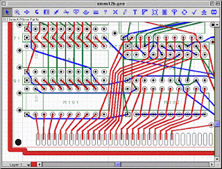
Is a flexible tool for designing printed circuit boards. It runs on Macintosh. Its many features include: virtually unlimited board sizes, number of board layers, number of parts, and support for both through-hole and surface mount parts and more.


 BSch3V
Is a schematic capture program for Windows. The name “BSch” is an abbreviation of “Basic Schematic”. It has only basic functions, in order to simplify operation.


 ExpressPCB
Is a snap to learn and use. Laying out PCBs is easy, even for the first time user.


 Kicad
Is an open source (GPL) software for the creation of electronic schematic diagrams and printed circuit board artwork. It is useful for everybody working in electronic design (schematic diagrams and Printed Board up to 16 layers).


 gEDA
Runs on Linux and has produced tools which are used for electrical circuit design, schematic capture, simulation, prototyping, and production. Currently, the gEDA project offers a mature suite of free software applications for electronics design; including schematic capture, attribute management, bill of materials (BOM) generation, netlisting into over 20 netlist formats, analog and digital simulation, and printed circuit board (PCB) design layout.


 Fritzing
Fritzing software is an interesting open-source initiative to support designers, artists, researchers and hobbyists to work creatively with interactive electronics and develop electronic projects. Fritzing helps you learn more about electronic circuits, to document your projects and even let’s you prepare them for production.


10  DesignSpark PCB
DesignSpark PCB is the world’s most accessible electronics design software. Easy to easy to learn and easy to use, it is designed to significantly reduce your concept-to-production time. At the core of this unique approach is a powerful software engine that enables you to capture Schematics, design PCB boards and layouts.


Baggio WANG FAN
-----------------------------------------------------------
SHENZHEN JAAPSON TECHNOLOGY CO LTD
Building 2, Tongfuyu Industrial Park,Shenzhen, China, 518104
Tel: 86-755-82596922
Fax:86-755-82596922/82596923
skype: baggiowang0214
baggio.wang@funsunpcb.com
baggio@jaapson-pcb.com
www.jaapsonpcb.com

JAAPSON, The Expert in HDI Multi-layer PCBs