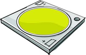
COB
(known as Chip-on-Board) is semi-conductor assembly technology where micro-chip
also known as die is electrically interconnected instead of using traditional
assembly process or individual IC packaging on the final product board. The
general term meaning of this technology is direct chip attachment also
refereeing to DCA. In DCA many kinds are available as substrate in form of
ceramic glass or ceramic substrate which has substances of excellent dielectric
and thermal property. It is also available in form of flex substrate, which
exhibits bendable ability. Other names are known as COG (chip-on-glass) or COF
(chip-on-flex).
COB
process consists of three main categories to perform when manufacturing the
Chip-on-Board. The first process is 'die mount or die attach', the second is
'wire bonding' and lastly 'the encapsulation of die wires'.

In
many COB assembly technology, FCOB(flip-chip-on-board) have chips facing
downward on the board and does not require wire bonding which employs chip
which the bond pads are pop up and it connects directly to pads on the board.
It is necessary to underfill flip-chip on active surface to protect bumps from
chemical and thermo-mechanical damage.
In
context of COB manufacturing process, 1) 'die attach' consists of applying die
attach holding to board or substrate mounting chip or die over die attach
materials. 2) For wire bonding, thermosonic (Au or Cu) ball bending and
ultrasonic (Al) wedge bending are used to connect wires between die and
substrate. Last part the encapsulation is done dispensing chemical liquid
(usually epoxy) over die and wires. Die and bond wires are encapsulated to
protect chemical and mechanical damage.
The advantages of COB include:
Better performance due to deceased interconnection between length and resistance.
And better protection against reverse engineering;
Reduced space and cost;
Shorter time to the market.
Higher reliability with better heat dispatch and small number of solder joint.
Better performance due to deceased interconnection between length and resistance.
And better protection against reverse engineering;
Reduced space and cost;
Shorter time to the market.
Higher reliability with better heat dispatch and small number of solder joint.
Applications
LED Backlight for LCD TV
LED Front light for E-Book
Agriculture & Horticulture Lighting
Street & Parking Lot Lighting
Invention
Reflective Pocket in PCB for LED Die Attachment (COB)
Patent pending
Advantages
Improved output efficiency of LED lighting
Avoid photonic absorption and scattering over the pocket wall
LED Backlight for LCD TV
LED Front light for E-Book
Agriculture & Horticulture Lighting
Street & Parking Lot Lighting
Invention
Reflective Pocket in PCB for LED Die Attachment (COB)
Patent pending
Advantages
Improved output efficiency of LED lighting
Avoid photonic absorption and scattering over the pocket wall
Baggio WANG FAN
-----------------------------------------------------------
SHENZHEN JAAPSON TECHNOLOGY CO LTD
Building 2, Tongfuyu Industrial Park,Shenzhen, China, 518104
Tel: 86-755-82596922
Fax:86-755-82596922/82596923
skype: baggiowang0214
baggio.wang@funsunpcb.com
baggio@jaapson-pcb.com
www.jaapsonpcb.com
-----------------------------------------------------------
SHENZHEN JAAPSON TECHNOLOGY CO LTD
Building 2, Tongfuyu Industrial Park,Shenzhen, China, 518104
Tel: 86-755-82596922
Fax:86-755-82596922/82596923
skype: baggiowang0214
baggio.wang@funsunpcb.com
baggio@jaapson-pcb.com
www.jaapsonpcb.com
JAAPSON, The Expert in HDI Multi-layer PCBs

