2015年9月7日星期一

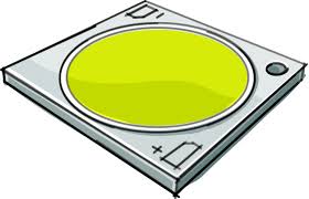
The Advantages of COB technology in LED


COB (known as Chip-on-Board) is semi-conductor assembly technology where micro-chip also known as die is electrically interconnected instead of using traditional assembly process or individual IC packaging on the final product board. The general term meaning of this technology is direct chip attachment also refereeing to DCA. In DCA many kinds are available as substrate in form of ceramic glass or ceramic substrate which has substances of excellent dielectric and thermal property. It is also available in form of flex substrate, which exhibits bendable ability. Other names are known as COG (chip-on-glass) or COF (chip-on-flex).


COB process consists of three main categories to perform when manufacturing the Chip-on-Board. The first process is 'die mount or die attach', the second is 'wire bonding' and lastly 'the encapsulation of die wires'. 


In many COB assembly technology, FCOB(flip-chip-on-board) have chips facing downward on the board and does not require wire bonding which employs chip which the bond pads are pop up and it connects directly to pads on the board. It is necessary to underfill flip-chip on active surface to protect bumps from chemical and thermo-mechanical damage.


 In context of COB manufacturing process, 1) 'die attach' consists of applying die attach holding to board or substrate mounting chip or die over die attach materials. 2) For wire bonding, thermosonic (Au or Cu) ball bending and ultrasonic (Al) wedge bending are used to connect wires between die and substrate. Last part the encapsulation is done dispensing chemical liquid (usually epoxy) over die and wires. Die and bond wires are encapsulated to protect chemical and mechanical damage.


The advantages of COB include:
Better performance due to deceased interconnection between length and resistance.
And better protection against reverse engineering;
Reduced space and cost;
Shorter time to the market.
Higher reliability with better heat dispatch and small number of solder joint.


Applications
LED Backlight for LCD TV
LED Front light for E-Book
Agriculture & Horticulture Lighting
Street & Parking Lot Lighting

Invention
Reflective Pocket in PCB for LED Die Attachment (COB)
Patent pending

Advantages
Improved output efficiency of LED lighting
Avoid photonic absorption and scattering over the pocket wall


Baggio WANG FAN
-----------------------------------------------------------
SHENZHEN JAAPSON TECHNOLOGY CO LTD
Building 2, Tongfuyu Industrial Park,Shenzhen, China, 518104
Tel: 86-755-82596922
Fax:86-755-82596922/82596923
skype: baggiowang0214
baggio.wang@funsunpcb.com
baggio@jaapson-pcb.com
www.jaapsonpcb.com
JAAPSON, The Expert in HDI Multi-layer PCBs

2015年9月1日星期二

Best of Free PCB Design Software


Do you need a free PCB design software or tool to put in practice the new electronic project you’ve just designed? So, we present you 10 of the best PCB software tools available on the internet that will help you to develop your printed circuit board faster and with ease.


  PCBWeb Designer
PCBWeb is a free CAD application for designing and manufacturing electronics hardware. Design multi-sheet schematics with our fast and easy-to-use wiring tool. Route multi-layer boards with support for copper pours and DRC checking. Integrated Digi-Key Parts Catalog with Bill of Materials Manager.


 ZenitPCB
Is an excellent pcb layout design software tool to create professional printed circuit board (PCB). It is flexible and easy to use CAD program, which allow you to realize your projects in a short time. With ZenitPCB Layout is possible to create the project starting both from the schematic capture or by the layout itself.


 FreePCB
Is a free, open-source PCB design editor for Microsoft Windows. It was designed to be easy to learn and easy to use, yet capable of professional-quality work. Some of its features are: 1 to 16 copper layers, board size up to 60 inches by 60 inches, imports and exports PADS-PCB netlists and more


 TinyCAD
Is a program to help you draw circuit diagrams. It comes complete with symbol libraries to get you started straight away. As well as being able to simply print your designs, you can use TinyCAD to publish your drawings by copying and pasting into a Word document or saving as a PNG bitmap for the web.


 Osmond PCB
Is a flexible tool for designing printed circuit boards. It runs on Macintosh. Its many features include: virtually unlimited board sizes, number of board layers, number of parts, and support for both through-hole and surface mount parts and more.


 BSch3V
Is a schematic capture program for Windows. The name “BSch” is an abbreviation of “Basic Schematic”. It has only basic functions, in order to simplify operation.


 ExpressPCB
Is a snap to learn and use. Laying out PCBs is easy, even for the first time user.


 Kicad
Is an open source (GPL) software for the creation of electronic schematic diagrams and printed circuit board artwork. It is useful for everybody working in electronic design (schematic diagrams and Printed Board up to 16 layers).


 gEDA
Runs on Linux and has produced tools which are used for electrical circuit design, schematic capture, simulation, prototyping, and production. Currently, the gEDA project offers a mature suite of free software applications for electronics design; including schematic capture, attribute management, bill of materials (BOM) generation, netlisting into over 20 netlist formats, analog and digital simulation, and printed circuit board (PCB) design layout.


 Fritzing
Fritzing software is an interesting open-source initiative to support designers, artists, researchers and hobbyists to work creatively with interactive electronics and develop electronic projects. Fritzing helps you learn more about electronic circuits, to document your projects and even let’s you prepare them for production.


10  DesignSpark PCB
DesignSpark PCB is the world’s most accessible electronics design software. Easy to easy to learn and easy to use, it is designed to significantly reduce your concept-to-production time. At the core of this unique approach is a powerful software engine that enables you to capture Schematics, design PCB boards and layouts.


Baggio WANG FAN
-----------------------------------------------------------
SHENZHEN JAAPSON TECHNOLOGY CO LTD
Building 2, Tongfuyu Industrial Park,Shenzhen, China, 518104
Tel: 86-755-82596922
Fax:86-755-82596922/82596923
skype: baggiowang0214
baggio.wang@funsunpcb.com
baggio@jaapson-pcb.com
www.jaapsonpcb.com

JAAPSON, The Expert in HDI Multi-layer PCBs

2015年8月10日星期一

Wireless communication: Jaapson PCB


Wireless communication is the transfer of information between two or more points that are not connected by an electrical conductor.


The most common wireless technologies use radio. With radio waves distances can be short, such as a few meters for television or as far as thousands or even millions of kilometers for deep-space radio communications. It encompasses various types of fixed, mobile, and portable applications, including two-way radios, cellular telephones, personal digital assistants (PDAs), and wireless networking. Other examples of applications of radio wireless technology include GPS units, garage door openers, wireless computer mice, keyboards and headsets, headphones, radio receivers, satellite television, broadcast television and cordless telephones.


Somewhat less common methods of achieving wireless communications include the use of other electromagnetic wireless technologies, such as light, magnetic, or electric fields or the use of sound.


Lisa LIU
SHENZHEN JAAPSON TECHNOLOGY CO LTD
Building 2, tongfuyu Industrial park, Shenzhen China, 518104
Tel: 86-755-82596922 Fax: 86-755-8259 6922 or 6923
lisa@jaapson-pcb.com
www.Jaapsonpcb.com
skype: jaapsoncircuits
Jaapson, Expert in HDI multi-layer PCB manufacturing

2015年8月5日星期三

Printed circuit board Jaapson


Baggio WANG FAN
-----------------------------------------------------------
SHENZHEN JAAPSON TECHNOLOGY CO LTD
Building 2, Tongfuyu Industrial Park,Shenzhen, China, 518104
Tel: 86-755-82596922
Fax:86-755-82596922/82596923
skype: baggiowang0214
baggio.wang@funsunpcb.com
baggio@jaapson-pcb.com
www.jaapsonpcb.com
JAAPSON, The Expert in HDI Multi-layer PCBs

2015年8月3日星期一

Carbon Conductive Ink: JAAPSON PCB


Carbon Conductive Ink is used to print contact areas on Contact Pad areas on e.g. Remote Control PCBs or on Mobile Phone PCBs (replacement of ENiG Surface Finish), to print switch contacts, shield areas, heating elements or as conductor in the cross over Technology (Crossing Tracks on single side PCBs).


At Jaapson PCB, we always use Atotech material: SD 2843. It has the below features and advantages:

Excellent definition due to optimized Rheology
Excellent adhesive strength and mechanical stability
Resistant during HASL
High chemical resistance
Protecting during plating processes by peelable soldermask


Baggio WANG FAN
-----------------------------------------------------------
SHENZHEN JAAPSON TECHNOLOGY CO LTD
Building 2, Tongfuyu Industrial Park,Shenzhen, China, 518104
Tel: 86-755-82596922
Fax:86-755-82596922/82596923
skype: baggiowang0214
baggio.wang@funsunpcb.com
baggio@jaapson-pcb.com
www.jaapsonpcb.com
JAAPSON, The Expert in HDI Multi-layer PCBs


2015年7月27日星期一

Vias Plated Shut with Copper

Vias Plated Shut with Copper
This is an older callout sometimes seen on legacy products. The original idea was to call for this as a way to have a copper conductive filled via. The problem with this process is that the holes must be extremely small to make this feasible since the copper used to to plate a via closed will also plate on all copper features on the board. (All vias and surface copper). Since 1oz of copper = 1.4mils, the amount of plating required to plate closed an 8 mil drilled hole is 2.8oz. 8mil/2 = 4 since plating is applied to both “sides” of the hole barrel. 4mil/1.4 = 2.85oz. This is 2.85oz additional copper to what is already on the surface of the board. This would bring the design’s total copper weight to 3.5 to 4oz. Tight space and trace designs are not possible with this amount of copper.

Another drawback is the extreme difficulty in plating the entire barrel of the hole evenly. A hole barrel will tend to plate faster toward the top and bottom of the hole which means a hole may look sealed but in the center there is trapped air and/or fluids which will outgas when exposed to assembly temperatures. We will not attempt this type of fill since far more reliable alternatives exist.


Baggio WANG FAN
-----------------------------------------------------------
SHENZHEN JAAPSON TECHNOLOGY CO LTD
Building 2, Tongfuyu Industrial Park,Shenzhen, China, 518104
Tel: 86-755-82596922
Fax:86-755-82596922/82596923
skype: baggiowang0214
baggio.wang@funsunpcb.com
baggio@jaapson-pcb.com
www.jaapsonpcb.com
JAAPSON, The Expert in HDI Multi-layer PCBs
Conductive vs Non-Conductive Filled Vias

Conductive vs Non-Conductive Filled Vias


Conductive Fill: Generally, a conductive filled via will be used when heat or a large amount of current needs to be carried from one side of the board to another. These can be found under chips that will be giving off a lot of heat where overheating is a concern. The metallic nature of the fill will naturally wick heat away from the chip to the other side of the board in many ways like a radiator.
The main drawback to conductive filled vias is the difference in CTE (Coefficient of Thermal Expansion) between the metallic fill and surrounding laminate. Metal will heat and expand much more rapidly than the surrounding laminate and this may cause fractures between the pads and hole wall. Because of this, conductive filled vias are not recommended for Via In Pad processing where the purpose of the fill is the reinforce the stability of the copper pad that is plated over the hole.


Non-Conductive Fill: A common misconception is that a non-conductive fill will either not pass any or only a very weak electrical signal through the via. This is not true. The barrels of the vias will still be plated with copper the same as any other via on the board, the only difference is the empty air in barrel is replaced with the fill material. This is usually done to prevent solder or other contaminants from entering the via or provide structural support for a copper pad covering the open hole in the case of a Via In Pad. Non-Conductive fill is another term for mask plugged vias.


Baggio WANG FAN
-----------------------------------------------------------
SHENZHEN JAAPSON TECHNOLOGY CO LTD
Building 2, Tongfuyu Industrial Park,Shenzhen, China, 518104
Tel: 86-755-82596922
Fax:86-755-82596922/82596923
skype: baggiowang0214
baggio.wang@funsunpcb.com
baggio@jaapson-pcb.com
www.jaapsonpcb.com
JAAPSON, The Expert in HDI Multi-layer PCBs