2015年7月27日星期一

Vias Plated Shut with Copper

Vias Plated Shut with Copper
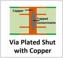
This is an older callout sometimes seen on legacy products. The original idea was to call for this as a way to have a copper conductive filled via. The problem with this process is that the holes must be extremely small to make this feasible since the copper used to to plate a via closed will also plate on all copper features on the board. (All vias and surface copper). Since 1oz of copper = 1.4mils, the amount of plating required to plate closed an 8 mil drilled hole is 2.8oz. 8mil/2 = 4 since plating is applied to both “sides” of the hole barrel. 4mil/1.4 = 2.85oz. This is 2.85oz additional copper to what is already on the surface of the board. This would bring the design’s total copper weight to 3.5 to 4oz. Tight space and trace designs are not possible with this amount of copper.

Another drawback is the extreme difficulty in plating the entire barrel of the hole evenly. A hole barrel will tend to plate faster toward the top and bottom of the hole which means a hole may look sealed but in the center there is trapped air and/or fluids which will outgas when exposed to assembly temperatures. We will not attempt this type of fill since far more reliable alternatives exist.


Baggio WANG FAN
-----------------------------------------------------------
SHENZHEN JAAPSON TECHNOLOGY CO LTD
Building 2, Tongfuyu Industrial Park,Shenzhen, China, 518104
Tel: 86-755-82596922
Fax:86-755-82596922/82596923
skype: baggiowang0214
baggio.wang@funsunpcb.com
baggio@jaapson-pcb.com
www.jaapsonpcb.com
JAAPSON, The Expert in HDI Multi-layer PCBs

Conductive vs Non-Conductive Filled Vias

Conductive vs Non-Conductive Filled Vias


Conductive Fill: Generally, a conductive filled via will be used when heat or a large amount of current needs to be carried from one side of the board to another. These can be found under chips that will be giving off a lot of heat where overheating is a concern. The metallic nature of the fill will naturally wick heat away from the chip to the other side of the board in many ways like a radiator.
The main drawback to conductive filled vias is the difference in CTE (Coefficient of Thermal Expansion) between the metallic fill and surrounding laminate. Metal will heat and expand much more rapidly than the surrounding laminate and this may cause fractures between the pads and hole wall. Because of this, conductive filled vias are not recommended for Via In Pad processing where the purpose of the fill is the reinforce the stability of the copper pad that is plated over the hole.


Non-Conductive Fill: A common misconception is that a non-conductive fill will either not pass any or only a very weak electrical signal through the via. This is not true. The barrels of the vias will still be plated with copper the same as any other via on the board, the only difference is the empty air in barrel is replaced with the fill material. This is usually done to prevent solder or other contaminants from entering the via or provide structural support for a copper pad covering the open hole in the case of a Via In Pad. Non-Conductive fill is another term for mask plugged vias.


Baggio WANG FAN
-----------------------------------------------------------
SHENZHEN JAAPSON TECHNOLOGY CO LTD
Building 2, Tongfuyu Industrial Park,Shenzhen, China, 518104
Tel: 86-755-82596922
Fax:86-755-82596922/82596923
skype: baggiowang0214
baggio.wang@funsunpcb.com
baggio@jaapson-pcb.com
www.jaapsonpcb.com
JAAPSON, The Expert in HDI Multi-layer PCBs

Via In Pad (Active Pad)

This process is becoming more and more common as BGA packages are becoming tighter. Rather than using the standard “dog bone” land pattern to transfer signal from the BGA footprint to a via that passes signal to other layers, vias can be drilled directly into the BGA footprint pads. This allows much simpler routing by soldering directly over the via. Make sure this process is called out in your fab notes.
TIP : We need to know the location, qty and size of the holes that need to be Via In Pad. The following steps are taken in this process.
  1. Drill the via (thru hole or blind)
  2. Fill the via with non-conductive material. Conductive material can be used but it’s not recommended since conductive material expands much more quickly than the surrounding laminate when heated which can cause cracks and pad failures during the assembly process.
  3. The surface of the plugged via is then plated over with copper.
  4. The newly plated copper surface is flattened and smoothed (planarized) to be even with the surrounding copper features.
  5. The final finish is applied
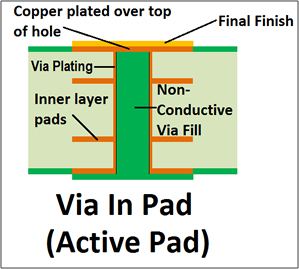
You now have a solderable surface mount pad that also passes signal to inner layers eliminating the need to rout the signal to a via on the surface layer.


Baggio WANG FAN
-----------------------------------------------------------
SHENZHEN JAAPSON TECHNOLOGY CO LTD
Building 2, Tongfuyu Industrial Park,Shenzhen, China, 518104
Tel: 86-755-82596922
Fax:86-755-82596922/82596923
skype: baggiowang0214
baggio.wang@funsunpcb.com
baggio@jaapson-pcb.com
www.jaapsonpcb.com
JAAPSON, The Expert in HDI Multi-layer PCBs

Mask (LPI) Plugged Vias (Non-Conductive Fill)

With a mask plugged via, (a.k.a. Mask Filled or Non-Conductive Filled via), specific measures are taken to ensure the via is plugged and sealed with mask and the annular ring is covered. A common application for this is on a BGA design where vias are commonly found in very close proximity to the BGA’s SMD pads. The concern is during assembly, solder will wick away from the intended pad and flow down the via creating poor or non-existent solder joints.


TIP: If you require mask plugged vias, this must be specified in your fab print or readme.txt file. We will need to know the quantity, sizes and locations of the vias to be plugged so we can be sure all the required holes are plugged.


Baggio WANG FAN
-----------------------------------------------------------
SHENZHEN JAAPSON TECHNOLOGY CO LTD
Building 2, Tongfuyu Industrial Park,Shenzhen, China, 518104
Tel: 86-755-82596922
Fax:86-755-82596922/82596923
skype: baggiowang0214
baggio.wang@funsunpcb.com
baggio@jaapson-pcb.com
www.jaapsonpcb.com
JAAPSON, The Expert in HDI Multi-layer PCBs
 

what is Via Tenting

This is the easiest and least costly process—actually there is no added cost for this process. Simply remove the mask clearances from the vias you wish to have tented. Tenting a via simply means to cover the annular ring and via hole with solder mask. No special steps are taken to ensure the hole opening remains closed. Tenting a via will sometimes result in the hole remaining covered but it isn't guaranteed. Smaller diameter vias (12mil diameter or less) ...have the best chance of remaining closed. The main purpose for tenting shouldn't be to close the opening of a hole but rather, cover the annular ring to prevent exposure to the elements and reduce accidental shorting or contact with the circuit.
 

TIP: If you are tenting some of the vias in your design, always make a fabrication note either in a readme.txt file or Gerber fab drawing so we know you have intentionally removed the mask clearances from some of your vias. Otherwise we may put the order on an engineering hold to verify your intention.


Baggio WANG FAN
-----------------------------------------------------------
SHENZHEN JAAPSON TECHNOLOGY CO LTD
Building 2, Tongfuyu Industrial Park,Shenzhen, China, 518104
Tel: 86-755-82596922
Fax:86-755-82596922/82596923
skype: baggiowang0214
baggio.wang@funsunpcb.com
baggio@jaapson-pcb.com
www.jaapsonpcb.com
JAAPSON, The Expert in HDI Multi-layer PCBs

2015年7月22日星期三

What is solder mask on PCB?


Solder mask or solder stop mask or solder resist is a thin lacquer-like layer of polymer that is usually applied to the copper traces of a printed circuit board (PCB) for protection against oxidation and to prevent solder bridges from forming between closely spaced solder pads. A solder bridge is an unintended electrical connection between two conductors by means of a small blob of solder. PCBs use solder masks to prevent this from happening. Solder mask is not always used for hand soldered assemblies, but is essential for mass-produced boards that are soldered automatically using reflow or solder bath techniques. Once applied, openings must be made in the solder mask wherever components are soldered, which is accomplished using photolithography.Solder mask is traditionally green but is now available in many colors.


Solder mask comes in different media depending upon the demands of the application. The lowest-cost solder mask is epoxy liquid that is silkscreened through the pattern onto the PCB. Other types are the liquid photoimageable solder mask (LPSM) inks and dry film photoimageable solder mask (DFSM). LPSM can be silkscreened or sprayed on the PCB, exposed to the pattern and developed to provide openings in the pattern for parts to be soldered to the copper pads. DFSM is vacuum laminated on the PCB then exposed and developed. All three processes go through a thermal cure of some type after the pattern is defined.


In electronic design automation, the solder mask is treated as a layer of the printed circuit board, and is described as a Gerber file like any other layer, such as the copper and silkscreen layers.


Available solder mask colors: Green, yellow, red, white, black, blue

 
Baggio WANG FAN
-----------------------------------------------------------
SHENZHEN JAAPSON TECHNOLOGY CO LTD
Building 2, Tongfuyu Industrial Park,Shenzhen, China, 518104
Tel: 86-755-82596922
Fax:86-755-82596922/82596923
skype: baggiowang0214
baggio.wang@funsunpcb.com
baggio@jaapson-pcb.com
www.jaapsonpcb.com

JAAPSON, The Expert in HDI Multi-layer PCBs

2015年7月13日星期一

Countersink Hole PCB


A countersink is a conical hole cut into a manufactured object, or the cutter used to cut such a hole. A common use is to allow the head of a countersunk bolt or screw, when placed in the hole, to sit flush with or below the surface of the surrounding material (by comparison, a counterbore makes a flat-bottomed hole that might be used with a socket-head cap screw).


A countersink may also be used to remove the burr left from a drilling or tapping operation thereby improving the finish of the product and removing any hazardous sharp edges.


The basic geometry of a countersink (cutter) inherently can be applied to the plunging applications described above (axial feed only) and also to other milling applications (sideways traversal). Therefore countersinks overlap in form, function, and sometimes name with chamfering end mills (endmills with angled tips). Regardless of the name given to the cutter, the surface being generated may be a conical chamfer (plunging applications) or a beveled corner for the intersection of two planes (traversing applications).


Baggio WANG FAN
-----------------------------------------------------------
SHENZHEN JAAPSON TECHNOLOGY CO LTD
Building 2, Tongfuyu Industrial Park,Shenzhen, China, 518104
Tel: 86-755-82596922
Fax:86-755-82596922/82596923
skype: baggiowang0214

JAAPSON, The Expert in HDI Multi-layer PCBs