- Drill the via (thru hole or blind)
- Fill the via with non-conductive material. Conductive material can be used but it’s not recommended since conductive material expands much more quickly than the surrounding laminate when heated which can cause cracks and pad failures during the assembly process.
- The surface of the plugged via is then plated over with copper.
- The newly plated copper surface is flattened and smoothed (planarized) to be even with the surrounding copper features.
- The final finish is applied
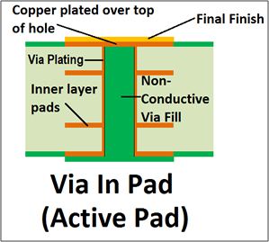 You now have a solderable surface mount pad that also passes signal to inner layers eliminating the need to rout the signal to a via on the surface layer.
Baggio WANG FAN
-----------------------------------------------------------
SHENZHEN JAAPSON TECHNOLOGY CO LTD
Building 2, Tongfuyu Industrial Park,Shenzhen, China, 518104
Tel: 86-755-82596922
Fax:86-755-82596922/82596923
skype: baggiowang0214
baggio.wang@funsunpcb.com
baggio@jaapson-pcb.com
www.jaapsonpcb.com
JAAPSON, The Expert in HDI Multi-layer PCBs
没有评论:
发表评论