2015年5月29日星期五

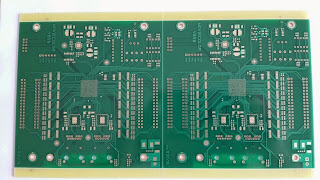
pcb lamination


Multi-layer printed circuit boards have trace layers inside the board. This is achieved by laminating a stack of materials in a press by applying pressure and heat for a period of time. This results in an inseparable one piece product. For example, a four-layer PCB can be fabricated by starting from a two-sided copper-clad laminate, etch the circuitry on both sides, then laminate to the top and bottom prepreg and copper foil. It is then drilled, plated, and etched again to get traces on top and bottom layers


Baggio WANG
SHENZHEN JAAPSON TECHNOLOGY CO LTD
Building 2, Tongfuyu Industrial Park,Shenzhen, China, 518104
Tel: 86-755-82596922
Fax:86-755-82596922/82596923
skype: baggiowang0214

JAAPSON, the special-tech PCB manufacturer for 10 years~

2015年5月26日星期二

SHENZHEN JAAPSON PCB Manufacturer

Shenzhen Jaapson Technology Co., Ltd, which was founded in 2004, is a high-tech enterprise specializing in designing, developing, manufacturing and marketing of Printed Circuit Board (PCB). We introduced advanced production and test equipment from overseas, professional engineering& management personnel and state-of-art technique to make sure we provide our customers with PCBs of high quality, reasonable price, fast delivery time and timely after-sales.

Through our continuous efforts and improvement, we are able to fully meet customers’ requirement for multi-layer, MCPCB, HDI PCB and high frequency PCBs, either for samples or mass production. They are widely used in such fields as telecommunications, medical, power supplies, military, computers, industrial, automobiles, LED lighting, etc.

We gained great popularity because of our responsibility, effectiveness and quality. We have established good partnership with many famous international companies and have strong customer base in North America, Europe, Asia, including sales agents worldwide. Our factories pass ISO9001, ISO14001, and our products meet UL, RoHS standards.

Our Mission: Exceed customers' expectations and offer better PCB Solutions all the time!


Our advantages:
Jaapson PCB was established in 2004, we have 10 year’s experience
We passed ISO9001, ISO14001, RoHS certificates
70% of our customers are from Europe and North America
We use very good material, such as KB, Shengyi, Rogers, Taiyo solder mask..
100% of our prodcuts are tested and 100% pass
Free samples are available for your test
Some of customers includes: CREE, WAGO, OSRAM, PHILIPS, BYD
We attend dozens of Electronics Fairs in Germany, USA, HK, etc
Our production line works 24hours without any break, to ensure timely delivery
We are golden member of CPCA and SECC.


Baggio WANG
-----------------------------------------------------------
SHENZHEN JAAPSON TECHNOLOGY CO LTD
Building 2, Tongfuyu Industrial Park,Shenzhen, China, 518104
Tel: 86-755-82596922
Fax:86-755-82596922/82596923
skype: baggiowang0214

2015年5月25日星期一

PCB Via holes


In printed circuit board design, a via consists of two pads in corresponding positions on different layers of the board, that are electrically connected by a hole through the board. The hole is made conductive by electroplating, or is lined with a tube or a rivet. High-density multi-layer PCBs may have microvias: blind vias are exposed only on one side of the board, while buried vias connect internal layers without being exposed on either surface. Thermal vias carry heat away from power devices and are typically used in arrays of about a dozen.


A via consists of:
  1. Barrel — conductive tube filling the drilled hole
  2. Pad — connects each end of the barrel to the component, plane or trace
  3. Antipad — clearance hole between barrel and metal layer to which it is not connected


A via may be at the edge of the board so that it is cut in half when the board is separated; this is known as a castellated hole and is used for a variety of reasons, including allowing one PCB to be soldered to another in a stack


Baggio WANG
-----------------------------------------------------------
SHENZHEN JAAPSON TECHNOLOGY CO LTD
Building 2, Tongfuyu Industrial Park,Shenzhen, China, 518104
Tel: 86-755-82596922
Fax:86-755-82596922/82596923

JAAPSON, the special-tech PCB manufacture

2015年5月24日星期日

What is HDI PCB

HDI is the abbreviation for High Density Interconnector. HDI PCB is defined as a PCB with a higher wiring density per unit area than conventional PCB. They have finer lines and spaces, smaller vias and capture pads and higher connection pad density than employed in conventional PCB technology. HDI PCB is used to reduce size and weight, as well as to enhance electrical performance of the device. HDI PCB is made through Microvia and buried vias and sequential lamination with insulation materials and conductor wiring for higher density of routing. HDI PCB is the best alternative to high layer-countand expensive standard laminate or sequentially laminated boards.

Concerning the electrical requirements for high-speed signal, the PCB must possess some AC characteristics, such as impedance control, high-frequency transmission capability and reduce unnecessary radiation. Multi-layered design is necessary for the structure of Stripline and Microstrip. In order to lesson the quality issues of signal transmission, the insulating material with low dielectric factor and low attenuation ratio is applied. Duo to the miniaturization and arrays of the electronic components, the PCB must be improved in the density. Along with the outcome of the assembling methods of Ball Grid Array, Chip Scale Package and Direct Chip Attachment, the PCB is featured with unprecedented high-density. The hole with a diameter less than 150um is known as Microvia. It can improve the effectiveness of assembly and space utilization and so on. It’s also necessary for the miniaturization of electronic products.

There were a lot of different names for the PCB with such structures. For example, it was called SBU (Sequence Build up the Process) in European and American industry as the program production is in the constructive mode of sequence. It was called MVP (Microvia Process) in Japanese industry because the hole of such products is much smaller than the previous one. It was also called BUM (Build up Multilayer Board) because the traditional multilayer is known as MLB (Multilayer Board).In order to avoid confusion, IPC Printed Circuit Association proposed to call it HDI (High Density Interconnection Technology) as the common name, but it can not reflect the characteristics of the circuit board. So the majority in the PCB industry define such products as HDI PCB.

There are a lot of advantages with HDI PCB, such as small size, high speed and high frequency. It is the main components of personal computers, portable computers, mobile phones and personal digital assistants. At present, except mobile phones, HDI PCB is also widely used in a variety of other consumer products, such as game consoles and MP3, etc. In addition, the applying of HDI PCB in notebook computer is expected trend since 2006 is in the industry.


SHENZHEN JAAPSON TECHNOLOGY CO LTD
Building 2, Tongfuyu Industrial Park,Shenzhen, China, 518104
Tel: 86-755-82596922
Fax:86-755-82596922/82596923
skype: baggiowang0214


JAAPSON, the special-tech PCB manufacturING for 10 years

2015年5月22日星期五

2 Layer aluminum PCB


Two (Double) layer MCPCB is consisting of two layers of copper conductor, put them on same side of metal core (usually aluminum, copper or iron alloy). The metal base is on the bottom of whole MCPCB, which is different from double sided MCPCB (the two copper layers were put on the each side of metal core respectively), and you can only populate SMD on top side.

Different from Single layer MCPCB, 2 layers MCPCB requires an additional pressing step to laminate the imaged thermal conductive laminate and metal core (also known as metal base) together.

Compared with normal FR4, this sturcture need more technology and experience on laminating of two layers together with metal core.

The processing steps of the MCPCB with the metal base embedded in the PCB are comparatively complex as hole plugging is required after primary drilling on the metal base in order to isolate it from the circuitry.


Capability of 2L MCPCB


•Base material: Aluminum/Copper/Iron Alloy
•Thermal Conductivity (dielectrial layer): 0.8, 1.5, 2.0, 3.0 W/m.K.
•Board Thickness: 0.5mm~3.0mm(0.02"~0.12")
•Copper thickness: 0.5 OZ, 1.0 OZ, 2.0 OZ, 3.0 OZ
•Outline: Routing, punching, V-Cut
•Soldermask: White/Black/Blue/Green/Red Oil
•Legend/Silkscreen Color: Black/White
•Surface finishing: Immersion Gold, HASL, OSP
•Max Panel size: 600*500mm(23.62"*19.68")
•Packing: Vacuum/Plastic bag
•Samples L/T: 5~7 Days
•MP L/T: 6~8 Days


Baggio WANG FAN
SHENZHEN JAAPSON TECHNOLOGY CO LTD
Building 2, Tongfuyu Industrial Park,Shenzhen, China, 518104
Tel: 86-755-82596922
Fax:86-755-82596922/82596923
SKYPE: BAGGIOWANG0214
baggio.wang@funsunpcb.com
baggio@jaapson-pcb.com
www.jaapsonpcb.com

Chip-On-Board-PCB


COB MCPCB, known as "Chip-On-Board" Metal Core PCB, is a type of MCPCB used in thermoelectric separation application. By using COB MCPCB, the micro-chip (also known as "die") directly touch the metal core where the heat dissipate, and electrically interconnect the trace of circuit board (wire-bonding) so that power supply can be provided.

In normal MCPCB, there's a dielectric layer between trace copper and metal core, and the thermal conductivity is limited by that dielectric layers, so value can only be 1~3 W/m.K. But using COB MCPCB, there's no such dielectric layer because chip (die) direct touch the metal core, so thermal conductivity value of COB MCPCB will be almost the same one of metal core material itself. The normal material of metal core is aluminum, so thermal conduviity of COB MCPCB is more than 200W/m.K.

COB process consists of three main categories to perform when manufacturing the Chip-on-Board:

1st: 'die mount or die attach';
2nd: 'wire bonding';
3rd: 'the encapsulation of die wires'.

By using wire bonding & epoxy packaging then directly embedded on MCPCB, this practice can extend the lifespan of LED and unified light emission.

According to process and material, COB MCPCB applications can be categorized into two types: Mirror Aluminum and silver or gold platting aluminum, or silver plating mirror aluminum PCB.


Advantage of utilizing COB MCPCB
•Excellent heat dissipation
•High thermal conductivity: 137W/m.K
•Higher reliability with better heat dispatch and small number of solder joint.
•Provide enhanced reliability and lifespan of LED
• Easy assembly for high powers LEDs
• High quality material and production process allows easy assembly and substantial reduce the error percentage in assembly process
•Substantially reduced space and cost
•With better security protection(difficult to hack using reverse engineering)
•Shorter time to the market


Application of COB MCPCB
•High Power LED (up to 200W)
• LED Backlight for LED TV
•LED Front Light for E-Book
•Agriculture & Horticulture Lighting
•Street & Parking Lot Lighting
•Automotive
•Power Supply
•ustomer Electronics Lighting
•Other products that require thermal solutions


Baggio WANG
-----------------------------------------------------------
SHENZHEN JAAPSON TECHNOLOGY CO LTD
Building 2, Tongfuyu Industrial Park,Shenzhen, China, 518104
Tel: 86-755-82596922
Fax:86-755-82596922/82596923
SKYPE: BAGGIOWANG0214
baggio.wang@funsunpcb.com


JAAPSON, the special-tech PCB manufacture

2015年5月21日星期四

What is OSP


What are the advantages using OSP surface finish?

What precautions should we take when using circuit boards supplied with OSP finish?

The biggest advantage of an OSP finished board is the price. OSP boards tend to be cheaper than those fabricated with other surfaces such as HASL, Immersion Tin, Immersion Silver or ENIG. Another advantage that OSP has, particularly as compared to HASL finished boards, is the flatness of the pads.

The primary drawbacks are related to solderability, shelf life, re-use of misprinted boards, and multiple heating cycles. The solderability/shelf life issues are connected; if the OSP degrades through shelf life (typically less than 1 year), the Copper underneath oxidizes fairly easily and prevents the board from being generally easy to solder.

The re-use of misprinted boards can also be an issue with OSP since alcohol and other solvents used to clean misprinted boards will also remove the OSP, leaving the Copper surface very easy to oxidize. Misprinted boards that are cleaned need to be sent back through the print/place/reflow processes quickly to avoid this issue.

Finally, OSP boards can be susceptible to solderability problems when subjected to multiple heating cycles; this occurs as a result of the OSP itself being degraded by the heating processes.


SHENZHEN JAAPSON TECHNOLOGY CO LTD
Building 2, Tongfuyu Industrial Park,Shenzhen, China, 518104
Tel: 86-755-82596922
Fax:86-755-82596922/82596923

What is Immersion Silver


IAg or Immersion Silver Plating is a surface plating technology used for Printed Circuit Boards. It consists of a thin immersion silver plating over the copper traces.

Advantages of immersion silver:
Excellent surface planarity (compared to e.g. HASL)
Low High Frequency Signal loss due to skin effect

Disadvantages of immersion silver:
Rapid degradation of surface due to oxidation or contamination (with e.g. sulfur or chlorine)
Silver "whiskers" form across electrical potentials and short out components.


Baggio WANG
-----------------------------------------------------------
SHENZHEN JAAPSON TECHNOLOGY CO LTD
Building 2, Tongfuyu Industrial Park,Shenzhen, China, 518104
Tel: 86-755-82596922
15017916507
Skype: baggiowang0214
Fax:86-755-82596922/82596923

2015年5月20日星期三

HDI multi-layer PCB factory


Since 2010, We have been introducing advanced production and test equipment from overseas, professional engineering& management personnel and state-of-art technique to make sure we provide our customers with HDI multi layer PCBs of high quality, reasonable price, fast delivery time and timely after-sales.

Jaapson technology capability
4-16 layer PCB
impedance control
blind via, buried via
mixed FR-4+Rogers technology
3mil trace width and space
thick gold PCB


SHENZHEN JAAPSON TECHNOLOGY CO LTD
Building 2, Tongfuyu Industrial Park,Shenzhen, China, 518104
Tel: 86-755-82596922
Fax:86-755-82596922/82596923
JAAPSON, the special-tech PCB manufacture

What is ENEPIG pcb


ENEPIG is suitable for soldering, gold wire bonding, aluminum wire bonding and contact resistance. It is formed by the sequential deposition of electroless Ni (120 to 240 micro inches) followed by 2 to 10 micro inches of electroless Palladium with an immersion gold flash of 2 to 6 micro inches on the top.

What is ENEPIG?

ENEPIG or Electroless Nickel - Electroless Palladium - Immersion Gold is a surface finish for Printed Circuit Boards that has been around for a decade but is only recently coming back into vogue. The high price of palladium had kept it out of reach for most businesses. With the price of palladium now less than the price of gold, this surface finish becomes the best choice for wire bonding, ROHS assembly and just all boards overall. ENEPIG works well with lead free and conventional eutectic solder alloys (Eutectic means its 63% tin and 37% lead.) ENEPIG is called the "Universal" surface finish as it can be used for all assembly processes.


So why is ENEPIG the "universal" finish?
Excellent ROHS lead free and leaded solderability
  • Because palladium completely dissolves into the solder leaving an oxide free nickel surface which allows a reliable tin nickel inter metallic.
High wire bond pull strengths (aluminum wire: up to 10g; gold wire: up to 8g). .
  • After numerous tests, it holds high pull weights.
  • Good for aluminum wedge and gold ball bonding
Low contact resistance
  • Due to the controlled deposition of precious metals the electrical resistance is more uniform so it's easier to predict amperage.
Suitable for conductive adhesives
  • You can connect components without the use of solder.
Finish is corrosion resistant and pore-free
  • Multiple layers of metal provide a higher corrosion resistant coating.
Unlimited shelf life
  • Doesn't tarnish
Nickel acts a barrier layer to further reduce copper dissolution during wave solder, thus ensuring good solderability.
  • Nickel prevents the mixing of copper and solder.
ENEPIG delivers great solder joint strength with various alloys during multiple reflow soldering, especially SAC305. The middle palladium layer helps to stabilize and control the inner metallic layer. Because of the mixture, ENEPIG after testing showed amazing wire bonding, both with aluminum and gold.


Mr. Baggio Wang
SHENZHEN JAAPSON TECHNOLOGY CO LTD
Building 2, Tongfuyu Industrial Park,Shenzhen, China, 518104
Tel: 86-755-82596922
Fax:86-755-82596922/82596923
baggio.wang@funsunpcb.com

JAAPSON, the special-tech PCB manufacture

What is ENIG(immersion gold)?


Electroless nickel immersion gold (ENIG) is a type of surface plating used for printed circuit boards. It consists of an electroless nickel plating covered with a thin layer of immersion gold, which protects the nickel from oxidation.

ENIG has several advantages over more conventional (and cheaper) surface platings such as HASL (solder), including excellent surface planarity (particularly helpful for PCBs with large BGA packages), good oxidation resistance, and usability for untreated contact surfaces such as membrane switches and contact points.

Early ENIG processes suffered from reliability issues which caused the ENIG finish to separate from the copper pads, taking the parts with them. ENIG also does not wet as evenly or easily as HASL. In addition, a "black-pad" of nickel oxide would form during the immersion gold plating step, greatly reducing solder joint reliability. To remedy this, a layer of electroless palladium can be plated onto the nickel to create ENEPIG surface finish.
ENIG is a costlier finish, but offers the best characteristics for printed circuit boards. The process requires the most steps compared to other common finishing types.

The electroless nickel step is an auto-catalytic process that involves depositing nickel on the palladium-catalyzed copper surface. The reducing agent containing nickel ions must be replenished in order to provide proper concentration, temperature and pH levels necessary to create a consistent coating. During the immersion gold step, the gold adheres to the nickel plated areas through molecular exchange, which will protect the nickel until the soldering process. The gold thickness needs to meet certain tolerances to ensure that the nickel maintains its solderability.


SHENZHEN JAAPSON TECHNOLOGY CO LTD
Building 2, Tongfuyu Industrial Park,Shenzhen, China, 518104
Tel: 86-755-82596922
Fax:86-755-82596922/82596923

COB PCB technology


COB (known as Chip-on-Board) is semi-conductor assembly technology where micro-chip also known as die is electrically interconnected instead of using traditional assembly process or individual IC packaging on the final product board. The general term meaning of this technology is direct chip attachment also refereeing to DCA. In DCA many kinds are available as substrate in form of ceramic glass or ceramic substrate which has substances of excellent dielectric and thermal property. It is also available in form of flex substrate, which exhibits bendable ability. Other names are known as COG (chip-on-glass) or COF (chip-on-flex).

COB process consists of three main categories to perform when manufacturing the Chip-on-Board. The first process is 'die mount or die attach', the second is 'wire bonding' and lastly 'the encapsulation of die wires'. In many COB assembly technology, FCOB(flip-chip-on-board) have chips facing downward on the board and does not require wire bonding which employees chip which the bond pads are pop up and it connects directly to pads on the board. It is necessary to underfill flip-chip on active surface to protect bumps from chemical and thermo-mechanical damage.

In context of COB manufacturing process, 1) 'die attach' consists of applying die attach holding to board or substrate mounting chip or die over die attach materials. 2) For wire bonding, thermosonic (Au or Cu) ball bending and ultrasonic (Al) wedge bending are used to connect wires between die and substrate. Last part the encapsulation is done dispensing chemical liquid (usually epoxy) over die and wires. Die and bond wires are encapsulated to protect chemical and mechanical damage.

The advantages of COB include better performance due to deceased interconnection between length and resistance. And better protection against reverse engineering; Reduced space and cost; Shorter time to the market. Higher reliability with better heat dispatch and small number of solder joint.

Applications
LED Backlight for LCD TV
LED Front light for E-Book
Agriculture & Horticulture Lighting
Street & Parking Lot Lighting

Invention
Reflective Pocket in PCB for LED Die Attachment (COB)
Patent pending

Advantages
Improved output efficiency of LED lighting
Avoid photonic absorption and scattering over the pocket wall


SHENZHEN JAAPSON TECHNOLOGY CO LTD
Building 2, Tongfuyu Industrial Park,Shenzhen, China, 518104
Tel: 86-755-82596922
Fax:86-755-82596922/82596923